
Motivation for changes
Artifacts in Frequency Sweeps
The graph below shows a measurement taken using the V13 firmware via the pcLink Configuration Menu item, using the “raw” command to export bridge voltages from my MR300 analyser. I converted these voltages to |Z|, VSWR, R and X: ‘Converting Bridge Voltages to Impedance’. Both the VSWR and R curves show step changes that are clearly artifacts and not representative of the true test load impedance.
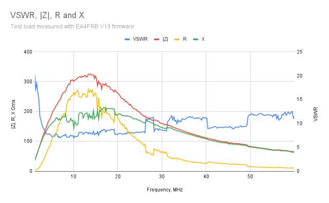
It can also be seen that the frequency sweeps are quite “noisy”, especially as impedance gets higher.
Measurement noise
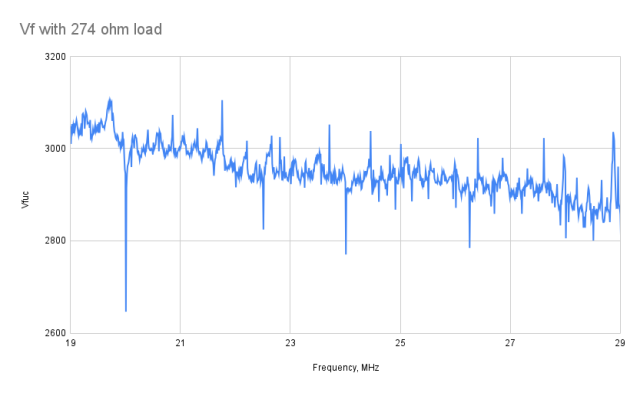
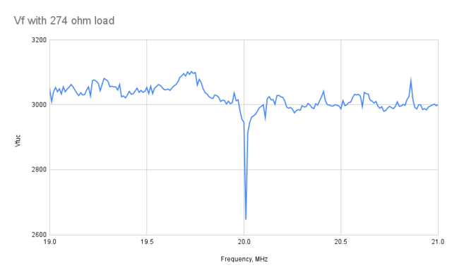
The graphs below show how Vf varies across a 10MHz frequency range when sampled at 10kHz intervals. The second chart is a zoom in to a 2MHz portion of that range.
The other voltages do vary in proportion, which reduces the noise feeding through to the calculated quantities VSWR, mod Z, R and X, but some noise inevitably passes through due to non-linearities and calibration errors.
The noise is quite repeatable, seeming to indicate that it originates in microcontroller noise and intermodulation between various harmonics of clock frequencies. In the MR300 clone, there is very little RF screening between the DDS chip & bridge voltage amplifiers and the microcontroller and the LCD module on the other side of the PCB. Adding some insulated copper strip behind the LCD has helped to reduce, but not eliminate this noise. The trick I use when making measurements is to select a step frequency such as 233 kHz, which means that measurement frequencies are unlikely to fall on whole multiples of clock frequencies.
High impedance loads and flatness
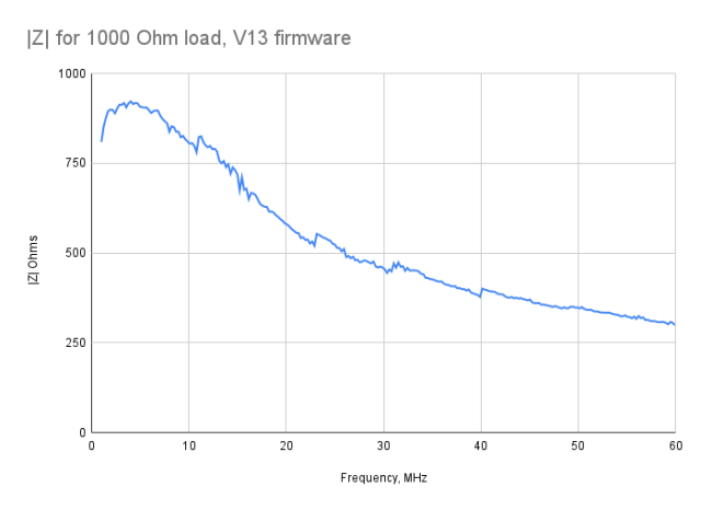
The figure below shows the uncorrected (calibration parameters not applied) results from a measurement of a 1000 ohm load. The very noticeable drop in measured impedance across frequency corresponds to the impedance of a small capacitance (around 10pF in order of magnitude) in parallel with the input, and is also noticeable on the open circuit load results. Were this a vector analyser, it would be relatively straightforward to determine the exact capacitance during calibration and remove it from the measured complex load impedance. This is not straightforward when the sign of Im(Z) is difficult to determine. However, it seemed likely that something could be done to at least partially remove this effect, given the existing calibration routine and knowledge of the causes. The second figure shows the effect in the corrected output of the V13 firmware.
Inductance and Capacitance modes show zero above 10MHz
Both the inductance and capacitance modes show zero at 10MHz and above, and I wanted to find out if this could be fixed.