Improved Measurement Artifacts
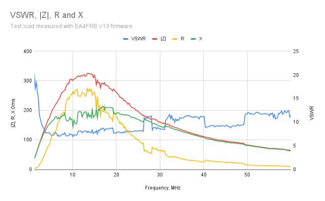
The reason for the step artifacts shown above seems to be a combination of
- the way that the V13 firmware compensates for the DDS output falling with frequency
- the V13 calibration methodology using stepwise changes in correction parameters with increasing frequency.
Either of these features in isolation can cause the steps, and the effects are worse in combination. When present together, the correction parameters not only vary in a stepwise manner, but when the DDS gain setting changes (again, this is stepwise) the “next” set of correction parameters not only pertain to the next frequency but also to a different DDS output level. This causes the changes to reflect nonlinearities in the voltage measurement circuits in addition to the step change in parameters.
In addition, at least on the MR300, there is insufficient internal screening between the DDS chip and bridge amplifiers, and the microcontroller and LCD module.
The graph below shows a measurement taken using the G1OJS V1.0 firmware.
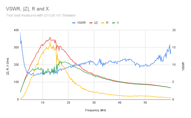
It can be seen that the ‘step’ artifacts present in the V13 results are gone (although significant noise remains), mainly thanks to keeping the DDS PGA output constant rather than changing it once per band.