Correcting Measurement Errors
The RF bridge voltages in the SARK100 and its clones are converted to DC voltages via diode detectors. The RF voltages are on the order of one or two volts peak to peak, and the diode response in this region is significantly nonlinear. Much of this nonlinearity can be removed by placing a matched diode in the feedback loop of the amplifier following the detector, and this technique is used to good effect. However, nonlinearities and offsets, both functions of frequency, remain in sufficient quantity to cause significant measurement errors if not further corrected numerically.
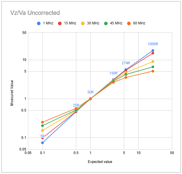
The graphs below show the ratios $V_z/V_a$ and $V_r/V_f$ for a range of load impedances and frequencies, before any numeric correction, as measured by my MR300 analyser. In each graph, the measured ratio is plotted on the vertical axis and the true expected value on the horizontal axis. A total lack of measurement errors would result in points spaced along the line through the origin with a slope of 1.
| Vz/Va, uncorrected | Vr/Vf, uncorrected |
|---|---|
 |
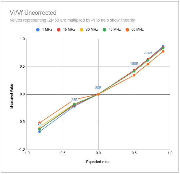 |
The ratio Va/Vz, which gives us the normalised magnitude of the load impedance, falls significantly at higher frequencies and load resistances. Similarly the ratio increases significantly at lower frequencies and lower load resistances. The behaviour with Vr/Vf (which gives the magnitude of the reflection coefficient) is less in magnitude but slightly more complicated; there is an overall scale factor where Vr/Vf measured is less than expected, and some variations with load impedance and frequency.
If these variations are not corrected numerically, in very rough terms, the error in impedance magnitude is in the range of roughly +/- 20% for resistive loads with an SWR in region around 3:1 to 5:1, and the error on the VSWR side is also around -20%. The VSWR error is significant because it leads to large errors in calculation of R and X even when the magnitude of Z is reasonably accurate.
Approach #1: Correcting bridge voltages
In the V13 firmware, EA4FRB uses a calibration process to determine coefficients for a function which yields a correction factor f as follows, where the subscripts on $V_t$ and $V_m$ denote V’true’ and V’measured’:
\[V_t = V_m f(V_m)\]The microcontroller in the SARK100 design has only 32kB of memory, so calculations are performed with integer data types and array sizes must be minimised. Hence, polynomial fitting is out of the question and a linear approximation is used for f, with coefficients being the usual $m$ and $c$ in $y=mx+c$.
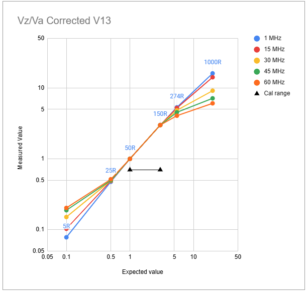
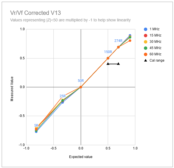
These coefficients are applied to the three independent voltages $V_r$, $V_z$ and $V_a$, and measured and tabulated at the centre of each frequency band. This gives excellent correction to the voltages at the calibration points, as can be seen in the graphs below. The graph for $V_z/V_a$ shows excellent results in the range $50<R_l<150$ and the graph for $V_r/V_f$ likewise in the range $50<R_l<274$. This is not surprising given that the coefficients for correcting $V_z$ and $V_a$ are determined from measurements at $R_l = 50$ and $R_l = 150$, and the coefficients for correcting $V_r$ are determined from measurements at $R_l = 150$ and $R_l = 274$.
However, the behaviours seen in the uncorrected graphs above remain, almost undiminished, in the corrected versions outside of these ranges. This means that accuracy falls off somewhat for load resistances significantly below 50 Ohms and above about 200 Ohms, especially at the higher frequencies.
Note that in this method, three loads are used (the open circuit case is only for setting DDS output level), and only two of the three loads are used to set each linear correction (50 and 150 for Vz and Va, 150 and 274 for Vr).
| Vz/Va, voltage correction | Vr/Vf, voltage correction |
|---|---|
 |
 |
Approach #2: Correcting bridge ratios
Whilst I had a little success with offsets and frequency interpolation in my initial code, I was sure that something better could be done and my mind kept going back to the two required and independent paths from bridge voltages to complex load impedance: the ratio $V_z/V_a$ and the ratio $V_r/V_f$. I was drawn to the idea of correcting these ratios instead of the component voltages, firstly because that’s two problems instead of three, and secondly because I realised that working with these ratios immediately eliminates a lot of the noise that is common to all four bridge voltages.
I had been playing with ideas for calibration models in spreadsheets based on frequency sweeps with about 250 rows of data (one per frequency point), and getting nice smooth results; hence, I really wanted a lookup table of calibration coefficients spaced only a few hundred kHz across the full range of 1MHz to 60MHz. But this wasn’t going to happen in 32kB of memory!
So, I decided to use linear interpolation between wider spaced calibration frequencies, as well as using a piecewise linear interpolation between calibration load values (and trying to keep the required number of loads as low as possible). I finally managed to squeeze in frequency calibration points spaced every 2 MHz (and independent from band centre and edge frequencies), and use four load resistances for calibration loads. Refactoring the code and avoiding arrays allowed me to squeeze this in to the memory available with some left over for new features. The correction function for each ratio is a simple mapping of $R_m$ (the measured ratio) to $R_t$ (the true ratio) using the linear interpolation formula:
\[R_t = R_{t1} + (R_{t2}-R_{t1})\frac{R_m - R_{c1}}{R_{c2}-R_{c1}}\]Where everything with a 1 or 2 in the subscript is a calibration measurement (m) or true known value (t) (e.g. VSWR=1.0:1 when Rl=50 Ohms). The formula looks a lot more complicated than it is; it simply asks a particular measured value how far it is proportionally along the line between two adjacent calibration measurement results, and then says “If you’re two thirds along the line between these measured calibration points, then you in reality are two thirds of the way along the line between these true values and your true value is therefore ….”.
Having said that the function is relatively simple, implementing it in integer arithmetic and being mindful of overflows and divide by zeros is all kinds of fun!
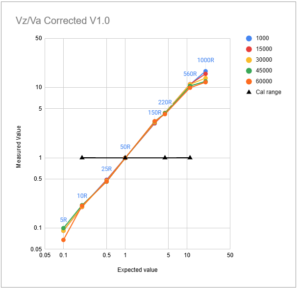
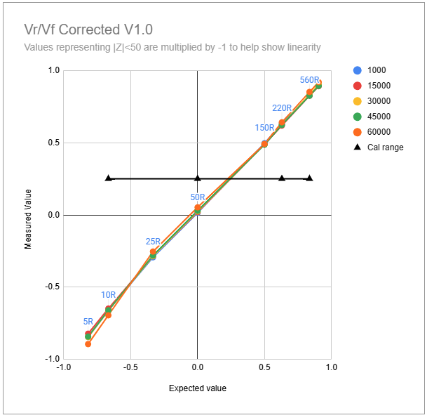
The results of this approach are shown in the two graphs below; not perfect, but the measured values stay closer to the true values especially at the extremes of frequency and load resistance. What this means for residual errors in the parameters that matter (Z, SWR, R and X) is shown here
Note that in this method, four loads are used (again, the open circuit case is only for setting DDS output level) and all four loads are used to set correction factors for both Vz/Va and Vr/Vf. (Hence, the difference between the two methods may be more a result of using four loads consistently vs using two different pairs of loads for the different corrections, than a result of correcting voltage ratios vs voltages).
| Vz/Va, ratio correction | Vr/Vf, ratio correction |
|---|---|
 |
 |